NanoContact Printing: Use of new Plastomers
Microcontact printing (µCP) is a simple and cost-effective method to create micrometer-scale chemical patterns on surfaces. By careful modification of the conventionally used stamping material (poly(dimethylsiloxane)-PDMS) and the stamping technique (e.g. “thin stamp µCP”) one can create surface chemical structures down to the submicron size-range. We have been investigating a new class of materials - polyolefin plastomers (POPs) for µCP applications. We have shown that the POP stamps are well suited to print proteins or block copolymers. Comparative studies on reproducibility, homogeneity and quality of printing between POP and conventional PDMS stamps have been performed and show a superior performance of the POP stamps in the nanometer range and an identical performance in the micrometer range compared to PDMS. Further advantages of the POP-based mCP are faster stamp production, the lack of monomeric contamination (typical for PDMS stamps) and the possibility of recycling the POP stamps. We believe that POPs offer a useful alternative to PDMS for µCP and open new possibilities in submicron-range printing.
Masters
The masters for the nanometer-range structures were fabricated using electron-beam lithography (EBL) by means of a Raith150 system (Raith GmbH, Dortmund, Germany): After cleaning, the samples were coated with a 200-nm thick polymethylmethacrylate (PMMA) layer (MicroChem Corp., Newton, USA) and hard baked for 60 min. at 180°C. The resist was then exposed with an acceleration voltage of 25 kV and an electron dose of 330 µC/cm2. The beam current was 13 pA. After exposure, the resist was developed in a methyl-isobutyl-ketone:isopropanol (MIBK:IPA) 1:3 solution for 60 s at 22°C and rinsed with pure isopropanol. After this lithographic step the samples were transferred to a dry etching plant 3 (Surface Technology Systems, STS T20, Ulm, Germany). The etching was performed with a mixture of 8 sccm CHF3 and 20 sccm SF6 at 41 mTorr, 300K and 55W for 3 minutes.
Formation of the stamps
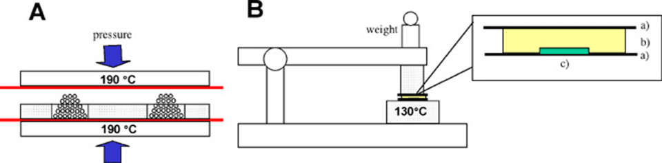
Affinity™ polyolefin plastomers were obtained as pellets from The Dow Chemical Company (Midland, MI, USA). The plastomers used (Affinity VP8770, Affinity EG8200, Affinity EG8150) are a relatively new class of polymers that emerged from recent developments in metallocene polymerization catalysts. POPs are copolymers of ethylene and an alpha-olefin such as butene or octene. The metallocene catalyst selectively polymerizes the ethylene and comonomer sequences. Increasing the comonomer content will produce polymers with higher elasticity as the comonomer incorporation disrupts the polyethylene crystallinity. Stamps (from all three Affinity POP variants) were produced as follows (see also Figure 1): The POP pellets were first melted into blocks of 40x20x5mm at 190°C under a pressure of 4 bars using an appropriate metal template. To avoid the sticking of the polymers to the heated metal planes, thin polyimide foils were placed in between. After cooling down to room temperature, the solid polymer bars were removed from the template, rinsed with ethanol and dried under a stream of nitrogen. In the next step the bars were placed over the stamp masters (10x10mm) and placed between two silicon wafers (50x30mm). This “sandwich” was then placed on a heatable plate (heated up to 130°C from both sides). First, a weight of 200g was put on the top of the sandwich for 5 minutes, which was afterwards increased to 700g for 4 minutes. After cooling, the master was easily peeled off from the POP bar, which was then cut to its proper size with a razor blade. Prior to usage, the POP stamps were cleaned with acetone for 5 minutes in an ultrasonic bath.
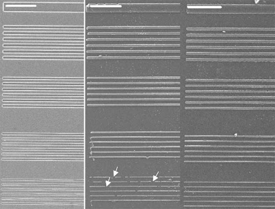
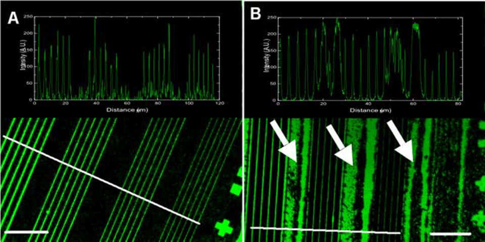
The ultimate test for a new stamping material is whether it is possible to ink it and transfer molecules to another substrate, replicating the master structure. We have tested the performance of the POP stamps by printing proteins (Alexa488-fibrinogen) and block copolymers (PLL-g-PEG-fl*) onto both glass and tissue-culture polystyrene (TCPS) surfaces using two different masters containing micrometer or submicron-sized structures. In each case, the results were compared to those obtained with conventional PDMS stamps.
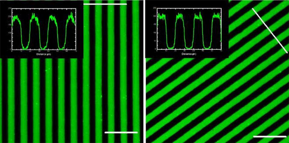
This is a typical example of a stamping experiment using the micrometer-range structures. There is no observable difference in the homogeneity and the quality of the printed structures between the POP (Affinity EG8150) and the PDMS printed surface. The protein-transfer ratio (from the stamp to the surface), as determined from the fluorescence intensities, was close to 100 % - there was no measurable fluorescence left on the stamps as observed by microscopy. The insets on the images show that in both cases the edges are well defined and there is no fluorescence present between the lines. The different POP variants all gave identical results (data not shown). After cleaned with ethanol (10 min in ultrasonic bath) both the POP and the PDMS stamps were reusable. In our tests we have reused the POP stamps at least 10 times without observing any changes in the printing quality.
perpendicular to the line directions. The lines across the stripes indicate the positions at which the cross sections were measured. Scale bars in the corners – 50 µm.
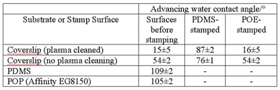
In order to test whether stamping modifies the properties (hydrophilicity/hydrophobicity) of the stamped surface, we have measured the advancing contact angles on the stamps and on the stamped surfaces. Non-printed substrates served as the reference. The stamps were in this case not inked, and non-structured (flat) stamps were used, but otherwise the printing was performed as described for the proteins, on normal glass coverslips, cleaned either only with ethanol/distilled water washing or by (in some cases) a subsequent oxygen plasma treatment. The results are summarized below .
The values in the table show that both stamp materials are rather hydrophobic. Upon contacting the surface, however, POP (Affinity EG8150) has no measurable effect on the contact angle, as compared to the control values. PDMS, on the other hand, significantly modifies the properties of the surface, making it hydrophobic. This indicates a contamination of the substrate by the stamp. The effect is stronger on the highly reactive (clean) plasma-treated surface and less pronounced (but still present) on the slightly contaminated ethanol-cleaned surface. A possible explanation for this fact could be that the residual organic contamination present on the glass surface reduces the PDMS contamination.
XPS measurements
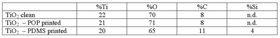
To obtain more information about possible surface contamination caused by the stamps, XPS measurements were also performed. The samples were prepared in a similar way to those used in contact angle measurements. Printing was again performed with flat/non-inked POP (Affinity EG8150) and PDMS, but in this case sputter coated (20nm) TiO2 surfaces were employed as substrates. Prior to printing, all substrates were cleaned by oxygen plasma treatment. The cleaning time was 2 minutes in the case of TiO2 surfaces and 10s in the case of stamps. The results of the XPS measurements of stamped TiO2 substrates were compared to those recorded on a non-stamped (clean) surface. Results are summarized below.
By analyzing the values we can conclude the following: the POP printing has no detectable effect on the surface composition of the substrate. In the event of contamination by the POP one would expect an increased amount of carbon on the surface but this was not observable. Si (as expected) is only detected in the case of PDMS stamping. This is a clear sign of monomeric PDMS contamination and has been previously reported. 12,13The increased carbon content may be also explained by the monomeric contamination.
We wish to thank Dr. Thomas Allgeuer of The Dow Chemical Company, Horgen, Switzerland, for supplying the polyolefin plastomers.